World's First Wafer-Level Camera Technology for Mobile Phones
19 June 2007 by axxxr
Tessera's solution is designed to overcome the cost, size and manufacturing roadblocks facing the industry as cameras become pervasive in mobile phones and other electronics. Using OptiML WLC technology, thousands of lenses are manufactured simultaneously on a wafer, and then bonded at the wafer level to create the optical element of the camera. The result is simplified assembly and up to 30% cost savings for the optical component of the camera module. OptiML WLC technology also reduces the size of the camera to a minimum, delivering up to 50% size reductions over conventional camera modules in camera phones today. Tessera's recently acquired Eyesquad technology can be easily integrated into the OptiML WLC solution, providing advanced auto-focus and digital optical zoom without the use of moving parts, resulting in greatly enhanced camera functionally and reliability at lower costs and smaller form factors. www.tessera.com 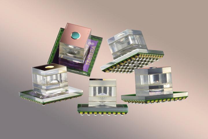 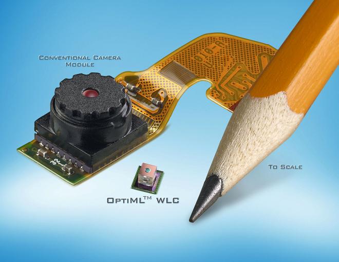 Comments On 23 Jun 04:28 chrris wrote now thats very clever, if it takes off it can be applied to al sorts of areas like cameras and camcorders and spy equipment, this could be B I G On 21 Jun 15:07 Belcompany wrote Lekker boeiend!! On 20 Jun 13:37 SiyalKhan wrote Great Work. On 20 Jun 08:56 SE4NICK wrote Excellent !!! On 19 Jun 23:56 Robert wrote Well it sounds great and all but i`m doutfull abaote its quality On 19 Jun 21:34 mcrosser wrote digital optical zoom without moving parts? what's that all about ! On 19 Jun 18:42 Phoenix wrote what about picture quality? On 19 Jun 18:02 seon wrote Hey man thats so cool - On 19 Jun 17:15 cardsnk wrote woah...thats so small... On 19 Jun 14:08 Jerry wrote Holy **** !!! its so small!! |


 RSS feed