| Author |
Camera Drivers Sony Ericsson for Series W/K/Z/VGA |
brazzuka's
Joined: Nov 14, 2007
Posts: > 500
From: South World-Antartida-Sweden
PM, WWW
|
IMAGE SENSORS IN SECURITY AND MEDICAL APPLICATIONS
Evgeny Artyomov, Alexander Fish, Orly Yadid-Pecht
Abstract: This paper briefly reviews CMOS image sensor technology and its utilization in security and medical
applications. The role and future trends of image sensors in each of the applications are discussed. To provide
the reader deeper understanding of the technology aspects the paper concentrates on the selected applications
such as surveillance, biometrics, capsule endoscopy and artificial retina. The reasons for concentrating on these
applications are due to their importance in our daily life and because they present leading-edge applications for
imaging systems research and development. In addition, review of image sensors implementation in these
applications allows the reader to investigate image sensor technology from the technical and from other views
as well.
Keywords: CMOS image sensors, low-power, security applications, medical applications.
ACM Classification Keywords: B.8.1.i Hardware - Integrated Circuits - Types and Design Styles - VLSI
1. Introduction
Fast development of low-power miniature CMOS image sensors triggers their penetration to various fields of our
daily life. Today we are commonly used to meet them in digital still and video cameras, cellular phones, web and
security cameras, toys, vehicles, factory inspection systems, medical equipment and many other applications
(see Figure 1). The advantages of current state-of-the-art CMOS imagers over conventional CCD sensors are the
possibility in integration of all functions required for timing, exposure control, color processing, image
enhancement, image compression and analog-to-digital (ADC) conversion on the same chip. In addition, CMOS
imagers offer significant advantages in terms of low power, low voltage, flexibility, cost and miniaturization. These
features make them very suitable especially for security and medical applications. This paper presents a review
of image sensors utilization in part of the security and the medical applications.
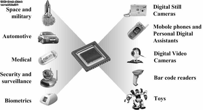
Figure 1. Image sensors applications
During the last few years imaging systems for security applications have been significantly revolutionising. Large,
high cost and inefficient cameras mostly used for specific military and government applications have been
replaced with compact, low-cost, low-power smart camera systems, becoming available not only for military and
government, but for wide spreading in civilian applications. In this paper we will concentrate on two major
categories: (a) surveillance systems � usually used for observation, anomaly detection and alarming, employing
one or multiple cameras, (b) biometrics systems � used for access control and person identification. Each of the
presented categories requires sensors having different specifications: for example, while low-power and
compactness are the most important features for some surveillance systems, robustness and high image quality
are the most important requirement in biometric systems.
Medical applications also benefit from the fast image sensors technology development. Introduction of miniature,
ultra-low power CMOS image sensors have opened new perspectives to minimally-invasive medical devices, like
wireless capsules for gastrointestinal tract observation [1]. Here we will review two very important medical
applications:
(a) artificial retina � used as an artificial replacement or aid to the damaged human vision system,
(b) wireless capsule endoscopy � used in minimally invasive gastrointestinal tract diagnostics.
The remainder of the paper is organized as follows: Section II briefly presents CMOS image sensor technology
with reference to "smart" CMOS image sensor architecture. The role of image sensors in security applications is
described in Section III. Section IV reviews medical applications employing state-of-the-art CMOS imagers.
Section V concludes the paper.
2. CMOS Image Sensor Technology in a Glance
The continuous advances in CMOS technology for processors and DRAMs have made CMOS sensor arrays a
viable alternative to the popular charge-coupled devices (CCD) sensor technology. Standard CMOS mixed-signal
technology allows the manufacture of monolithically integrated imaging devices: all the functions for timing,
exposure control and ADC can be implemented on one piece of silicon, enabling the production of the so-called
�camera-on-a-chip� [2]. Figure 2 is a diagram of a typical digital camera system, showing the difference between
the building blocks of commonly used CCD cameras and the CMOS camera-on-a-chip [3]. The traditional imaging
pipeline functions�such as color processing, image enhancement and image compression�can also be
integrated into the camera. This enables quick processing and exchanging of images. The unique features of
CMOS digital cameras allow many new applications, including network teleconferencing, videophones, guidance
and navigation, automotive imaging systems, robotic and machine vision and of course, security and bio-medical
image systems.
Most digital cameras still use CCDs to implement the image sensor. State-of-the-art CCD imagers are based on a
mature technology and present excellent performance and image quality. They are still unsurpassed for high sensitivity and long exposure time, thanks to extremely low noise, high quantum efficiency and very high fill
factors. Unfortunately, CCDs need specialized clock drivers that must provide clocking signals with relatively
large amplitudes (up to 10 V) and well-defined shapes. Multiple supply and bias voltages at non-standard values
(up to 15 V) are often necessary, resulting in very complex systems.
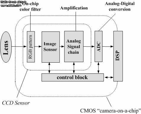
Figure 2. Block diagram
of a typical digital camera system.
Figure 3. Block diagram
of a typical interline transfer CCD image sensor.
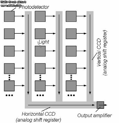
Figure 3 is a block diagram of a widely used interline transfer CCD image sensor. In such sensors, incident
photons are converted to charge, which is accumulated by the photodetectors during exposure time. In the
subsequent readout time, the accumulated charge is sequentially transferred into the vertical and horizontal
CCDs and then shifted to the chip-level output amplifier. However, the sequential readout of pixel charge limits
the readout speed. Furthermore, CCDs are high-capacitance devices and during readout, all the capacitors are
switched at the same time with high voltages; as a result, CCD image sensors usually consume a great deal of
power. CCDs also cannot easily be integrated with CMOS circuits due to additional fabrication complexity and
increased cost. Because it is very difficult to integrate all camera functions onto a single CCD chip, multiple chips
must be used. A regular digital camera based on CCD image sensors is therefore burdened with high power
consumption, large size and a relatively complex design; consequently, it is not well suited for portable imaging
applications.
Unlike CCD image sensors, CMOS imagers use digital memory style readout, using row decoders and column
amplifiers. This readout overcomes many of the problems found with CCD image sensors: readout can be very
fast, it can consume very little power, and random access of pixel values is possible so that selective readout of
windows of interest is allowed. The power consumption of the overall system can be reduced because many of
the supporting external electronic components required by a CCD sensor can be fabricated directly inside a
CMOS sensor. Low power consumption helps to reduce the temperature (or the temperature gradient) of both the
sensor and the camera head, leading to improved performance.
An additional advantage of CMOS imagers is that analog signal and digital processing can be integrated onto the
same substrate, allowing fabrication of so called "smart" image sensors. Many "smart" image sensors have
already been demonstrated in the literature. They performed functions of real time object tracking [4]-[11], motion
detection [12]-[13], image compression [14]-[15], widening the dynamic range of the sensor [16]-[20] and others.
These functions are usually performed by digital or nonlinear analog circuits and can be implemented inside the
pixels and in the periphery of the array. Offloading signal processing functions makes more memory and DSP
processing time available for higher-level tasks, such as image segmentation or tasks unrelated to imaging.
CMOS pixels can be divided into two main groups, passive pixel sensors (PPS and active pixel sensors (APS).
Each individual pixel of a PPS array has only a photosensing element (usually a photodiode) and a switching MOSFET transistor. The signal is detected either by an output amplifier implemented in each column or by a
single output for the entire imaging device. These conventional MOS-array sensors operate like an analog DRAM, offering the advantage of random access to the individual pixels. They suffer from relatively poor noise
performance and reduced sensitivity compared to state-of-the-art CCD sensors. APS arrays are relatively novel
image sensors that have amplifiers implemented in every pixel; this significantly improves the noise parameter
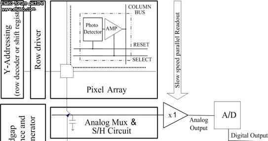
Figure 4. General architecture of the "smart" CMOS APS based image sensor.
Figure 4 shows the general architecture of the "smart" CMOS APS based image sensor. The core of this architecture is a camera-on-a-chip, consisting of a pixel array, a Y-addressing circuitry with a row driver, an Xaddressing
circuitry with a column driver, an analog front end (AFE), an analog-to-digital converter (ADC), a digital timing and control block, a bandgap reference and a clock generator.
Optional analog and digital processing blocks "upgrade" the camera-on-a-chip core to a "smart" imager, and they are used to perform
additional functions, that can vary from design to design, depending on the application and system requirements.
The basic imager operation, depends on the chosen photodetector and pixel types, readout mode, Y-addressing
and X-addressing circuitries, ADC type and of course, the analog and/or digital image processing. A brief description of the main imager building blocks is presented herein.
A. APS Pixel Array � the imager pixel array consists of N by M active pixels, while the most popular is the basic
photodiode APS pixel, employing a photodiode and a readout circuit of three transistors. Generally, many types of
photodetectors and pixels can be found in the literature. This includes a p-i-n photodiode, photogate and pinned
photodiode based pixels, operating either in rolling shutter or in global shutter (snapshot) readout modes. The difference between these modes is that in the rolling shutter approach, the start and end of the light collection for each row is slightly delayed from the previous row, leading to image distortion when there is relative motion between the imager and the scene.
On the other hand, the global shutter technique uses a memory element
inside each pixel and provides capabilities similar to a mechanical shutter: it allows simultaneous integration of
the entire pixel array and then stops the exposure while the image data is read out.
A detailed description of both rolling shutter and global shutter pixels can be found in [3]. Note, although most of today's "cameras-on-a-chip utilize" very simple pixels, many "smart" imagers employ more
complicated pixels. Some of them perform analog image processing tasks at the pixel level. Very good examples
for these imagers are neuromorphic sensors, where each pixel consists of a photo detector and local circuitry,performing spatio-temporal computations on the analog brightness signal. Another example is an imager, where
the A/D conversion is performed in the pixel level.
B. Scanning Circuitry � Unlike CCD image sensors, CMOS imagers use digital memory style readout, usually
employing Y-Addressing and X-Addressing to control the readout of output signals through the analog amplifiers
and allow access to the required pixel. The array of pixels is accessed in a row-wise fashion using the YAddressing
circuitry. All pixels in the row are read out into column analog readout circuits in parallel and then are
sequentially read out using the X-Addressing circuitry (see Figure 4).
C. Analog Front End (AFE) - all pixels in a selected row are processed simultaneously and sampled onto sampleand-
hold (S/H) circuits at the bottom of their respective rows. Due to this column parallel process, for an array
having M columns, the AFE circuitry usually consists of 2*M S/H circuits, M size analog multiplexer, controlled by
the X-Addressing circuitry, and one or M amplifiers to perform correlated double sampler (CDS). The CDS
improves the signal-to-noise ratio (SNR) by eliminating the fixed pattern noise (FPN). A programmable- (or
variable-) gain amplifier (PGA or VGA) follows the CDS to amplify the signal and better utilize the full dynamic
range of the A/D converter (ADC).The number of amplifiers, required to perform the CDS functionality depends
on the chosen CDS architecture and is equal to 2*N in case the subtraction is done separately for each column.
The choice of an AFE configuration depends on many factors, including: the type of sensor being used, dynamic
range, resolution, speed, noise, and power requirements. The considerations regarding making appropriate AFE
choices for imaging applications can be found in [21].
D. Analog-to-digital conversion (ADC) � ADC is the inherent part of state-of-the-art "smart" image sensors. There
are three general approaches to implementing sensor array ADC:
1. Pixel-level ADC, where every pixel has its own converter [22]-[23]. This approach allows parallel operation of
all ADCs in the APS array, so a very low speed ADC is suitable. Using one ADC per pixel has additional
advantages, such as higher SNR and simpler design.
2. Column-level ADC, where an array of ADCs is placed at the bottom of the APS array and each ADC is
dedicated to one or more columns of the APS array [24]-[25]. All these ADCs are operated in parallel, so a low-tomedium-
speed ADC design can be used, depending on the sensor array size. The disadvantages of this
approach are the necessity of fitting each ADC within the pixel pitch (i.e., the column width) and the possible
problems of mismatch among the converters at different columns.
3. Chip-level ADC, where a single ADC circuit serves the whole APS array [26]-[27]. This method requires a very
high-speed ADC, especially if a very large array is used. The architecture shown in Figure 4, utilizes this
approach for ADC implementation.
E. Bandgap reference and current generators � these building blocks are used to produce on-chip analog voltage
and current references for other building blocks like amplifiers, ADC, digital clock generator and others. It is very
important to design high precision and temperature independent references, especially in high resolution state-ofthe-
art image sensors, where the temperature of the die can vary by many tens of degrees.
F. Digital timing and control block, clock generator - aim to control the whole system operation. Their
implementation in the chip level decreases the number of required I/O pads and thus reduces system power
dissipation. Synchronized by the generated clock, the digital timing and control block produces the proper
sequencing of the row address, column address, ADC timing and the synchronization pulses creation for the pixel
data going offchip. In addition, it controls the synchronization between the imager and the analog and digital
processing.
G. Analog and Digital Image Processing � although these blocks are optional, they play a very important role in
today's "smart" image sensors. Conventional vision systems are put at a disadvantage by the separation between
a camera for �seeing� the world, and a computer or DSP for �figuring out� what is seen. In these systems all
information from the camera is transferred to the computer for further processing. The amount of processing
circuitry and wiring necessary to process this information completely in parallel is prohibitive. In all engineered
systems, such computational resources are rarely available and are costly in terms of power, space, and
reliability. Opposite to a conventional camera-on-a-chip, which only captures the image and transfer it for the
further processing, "smart" image sensors reduce the computational cost of the processing stages interfaced to it by carrying out an extensive amount of computation at the focal plane itself (analog and digital image processing
blocks in Figure 4), and transmitting only the result of this computation (see Figure 5)
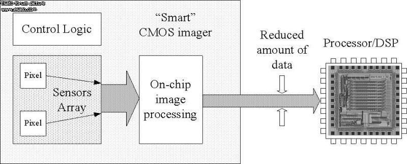
Figure 5. An example of an imaging system, employing a "smart" CMOS image sensor with on-chip processing
and processors/DSPs for image processing
Both analog and digital processing can be performed either in the pixel or in the array periphery. There are
advantages and disadvantages for both methods. In-pixel digital image processing is very rare because it
requires pixel-level ADC implementation and results in very poor fill factor and large pixel size. In-pixel analog
image processing is very popular, especially in the field of neuromorphic vision chips. In these chips in-pixel
computations are fully parallel and distributed, since the information is processed according to the locally sensed
signals and data from pixel neighbors. Usually, neuromorphic visual sensors have very low-power dissipations
due to their operation in the subthreshold region, but suffer from low resolution, small fill-factor and very low
image quality. Other applications employing in-pixel analog processing are tracking chips, wide dynamic range
sensors, motion and edge detection chips, compression chips and others. The periphery analog processing
approach assumes that analog processing is performed in the array periphery without penalty on the imager
spatial resolution and it is usually done in a column parallel manner. While this approach has computational
limitations compared to in-pixel analog processing, it allows better image quality. Periphery digital processing is
the most standard and usually simpler. It is performed following the A/D conversion, utilizes standard existing
techniques for digital processing and is usually done on the chip level. The main disadvantage of this approach is
its inefficiency by means of area occupied and power dissipation. Note, all mentioned techniques can be mixed
and applied together on one chip to achieve better results.
3. Image Sensors in Security Applications
The importance of security applications has significantly increased due to numerous terrorists� attacks worldwide.
This area also greatly benefits from the achievements in the image sensors field. Today we can meet the
cameras not only in military applications, but also in commercial and civilian applications. They are present in the
shops and on the streets, in the vehicles and on the robots. The applications are numerous and can not be
covered in this short paper. We have decided to concentrate on two important applications that represent a large
fraction of the total security market. These applications are surveillance and biometrics. Both of the applications
are extensively utilized in military, commercial and civilian fields.
3.1 Surveillance
Surveillance systems enable a human operator [28] to remotely monitor activity over large areas. Such systems
are usually equipped with a number of video cameras, communication devices and computer software or some
kind of DSP for real-time video analysis. Such analysis can include scene understanding, attention based
alarming, colour analysis, tracking, motion detection, windows of interest extraction etc. With recent progress in
CMOS image sensor technology and embedded processing, some of the mentioned functions and many others
can be implemented in dedicated hardware, minimizing system cost and power consumption. Of course, such integration affects system configurability, but not all applications require configurable systems: some of them benefit from low cost and low power dedicated hardware solutions.
For example, in [29] we have presented an image sensor that can be used for such applications. Due to a specific
scanning approach this sensor can be used efficiently for motion detection, tracking, windowing and digital zoom.
Figure 6 shows the standard approach for sensor data scan - raster and the alternative � Morton or Z scan.
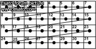
(a) raster scan � conventional approach in image
sensors,
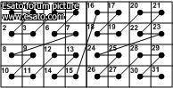
(b) Morton (Z) scan � newly proposed and
implemented
Figure 6. Two approaches for data scan
The Morton (Z) scan poses a very valuable feature, neighbor pixels that are concentrated in blocks appear at the
output sequentially, one after other. With this scanning approach the image blocks can be easily extracted and
processed with simple on-chip hardware. For example, for constructing video camera with �4 digital zoom, the
blocks of 4�4 pixels need to be extracted and averaged. Similarly, cameras with digital zoom �8 and �16 can be
easily constructed. Figure 7 shows measurements from our test chip.
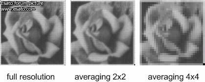
Figure 7. Morton scan chip test results
Another example is a wide dynamic range (WDR) imager. Dynamic range (DR) quantifies the ability of a sensor
to image highlights and shadows. If we define the dynamic range of the sensor as 20log(S/N), where S is the
maximal signal value and N is the sensor noise, the typical image sensors will have a very limited dynamic range,
about 65-75 dB. Wide dynamic range imaging is very important in many surveillance systems. The dynamic
range can be increased in two ways: the first one is noise reduction and thus enabling expansion of the dynamic
range toward darker scenes; the second method is incident light saturation level expansion, thus improving the
dynamic range toward brighter scenes.
Herein we present one of the possible solutions for dynamic range extension in CMOS Active Pixel Sensors
(APS) [2]. As in a traditional CMOS APS, this imager is constructed of a two-dimensional pixel array, with random
pixel access capability and row-by-row readout rolling shutter method. Each pixel contains an optical sensor to
receive light, a reset input and an electrical output representing the illumination received. This imager implements
a simple function for saturation detection, and is able to control the light exposure time on a pixel-by-pixel basis,
resulting in no saturation. The pixel value can then be determined as a floating-point representation. To do so, the
outputs of a selected row are read out through the column-parallel signal chain, and at certain points in time are
also compared with an appropriate threshold value, as shown in Figure 8. If a pixel value exceeds the threshold,
i.e. the pixel is expected to be saturated at the end of the exposure time; the reset is given at that time to that
pixel. The binary information concerning the reset (i.e., if it is applied or not) is saved in a digital storage for later
calculation of the scaling factor. Thus, we can represent the pixel output in the following floating-point format:M ⋅2EXP , where the mantissa (M) represents the digitized pixel value and the exponent (EXP) represents the scaling factor. This way a customized, linear, large increase in the dynamic range is achieved.
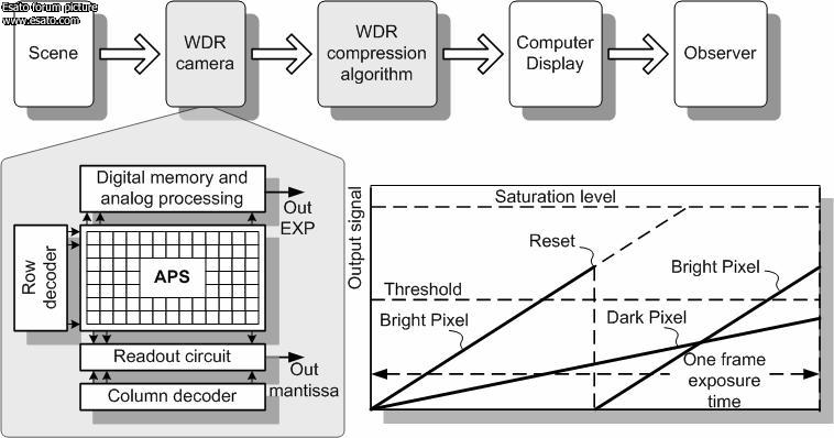
Figure 8. Imaging pipeline, image sensor architecture and work principle.
Figure 9(a) and Figure 9(b) show a comparison between an image captured by a traditional CMOS imager and by
the autoexposure system described here. In Figure 9(a), a scene is imaged with a strong light hitting the object;
hence, some of the pixels are saturated. At the bottom of Figure 9(b), the capability of the autoexposure sensor
for imaging the details of the saturated area in real time may be observed. Since the display device is limited to
eight bits, only the most relevant eight-bit part (i.e., the mantissa) of the thirteen-bit range of each pixel is
displayed here. The exponent value, which is different for different
areas, is not displayed.
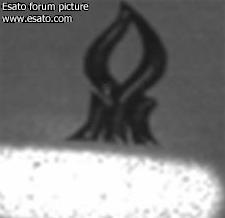
Figure 9. (a) Scene observed with a traditional
CMOS APS sensor,
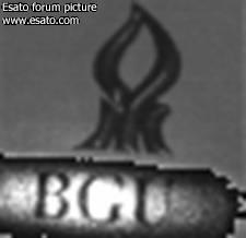
Figure 9. (b) Scene observed with our in-pixel
autoexposure CMOS APS sensor.
3.2 Biometric personal identification
Biometric personal identification is strongly related to security and it refers to �identifying an individual based on
his or her distinguishing physiological and/or behavioral characteristics (biometric identifiers)� [30]. Figure 10
shows the most frequently used biometric characteristics.
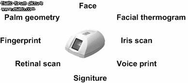
Figure 10. Biometric characteristics
Almost all biometric characteristics, shown in Figure 10, require some kind of sensing. Usually, conventional
image sensors with external hardware or software image processing are used. The difficulty for on-chip
integration is caused by the complexity of the required image processing algorithms. However, there are some
developments that successfully achieve the required goals by parallel processing utilization.
To give some more detailed examples in the field, we concentrate on fingerprint sensors. Generally these
sensors can be classified by the physical phenomena used for sensing: optical, capacitance, pressure and
temperature. The first two classes are the most popular and both mainly employ CMOS technology.
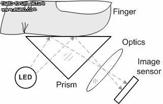
(a) optical - reflection based sensor
(b) optical � transmission based sensor
(c) non-optical � based on pressure,
capacitance or temperature sensor
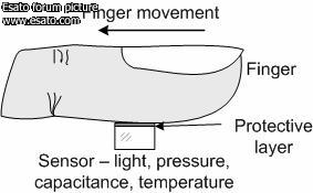
(d) �sweep� sensor
Figure 11. Fingerprint sensors
In Figure 11 various technologies for fingerprint sensing are shown [31]. The most popular approach (see Figure 11 (a)) is based on optical sensing and light reflection from the finger surface. Also, this type provides high robustness to finger condition (dry or wet), but the system itself is tend to be bulky and costly. Alternative
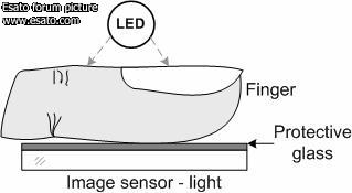
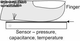
solutions that can provide compact and lower cost solutions, are based mostly on solid state sensors where the finger is directly placed on the sensor. However, in these solutions the sensor size needs to be at least equal to the size of the finger part used for sensing. Two sensors of this type are shown in Figure 11 (b) and (c).
The first one is based on light transmitted through the finger and then sensed by the image sensor, while the second one
is the non-optical sensor that can be implemented either as pressure, capacitance or temperature sensor. The fingerprint sensor, known as a �sweep� sensor and shown in Figure 11 (d), can be implemented using either the optical or other previously mentioned techniques. A �sweep� sensor employs only a few rows of pixels, thus in
order to get a complete fingerprint stamp the finger needs to be moved over the sensing part.
Such technology greatly reduces the cost of the sensor due to reduced sensor area and solves the problem of fingerprint stamp
that needs to be left on the surface in the first two methods.
In all presented methods, the output signal is usually an image and the sensors are composed of pixels that sense either temperature, pressure, photons or change in capacitance. The overall architectures of these sensors are similar to the architecture described in section II and they integrate various image and signal processing algorithms, implemented the same die. Various research papers have been published in this area and numerous companies are working on such integration. For example, in [32] the authors implement image enhancement and
robust sensing for various finger conditions. Capacitive sensing CMOS technology is used and data is processed in a column parallel way. The same technology is used also in [34], but the fingerprint identifier is also integrated and the data is processed massively in parallel for all pixels.
Despite the fact that fingerprint technology is quite mature, there is much work to be done to reduce power consumption, to improve technology and image processing algorithms and to achieve better system miniaturization.
4. Image Sensors in Medical Applications
Almost all medical and near medical areas benefit from image sensors utilization. These sensors are used for
patients� observation and drug production, inside the dentists offices and during surgeries. In most cases the
sensor itself represents only a small fraction (in size and cost) of the larger system, but its functionality plays a
major role in the whole system. Figure 12 shows examples of medical applications where CMOS image sensors
are used. In this section of the paper we mostly concentrate on applications that push current image sensor
technology to the edge of the possibilities. These applications are wireless capsule endoscopy and retinal
implants. Both of these applications will play an important role in millions of patients� lives in the near future.
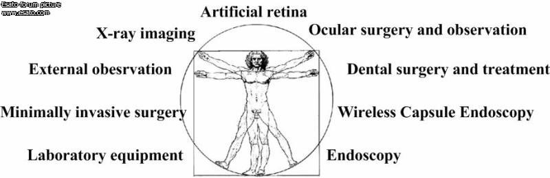
Figure 12. Image sensors applications in medicine
4.1 Wireless Capsule Endoscopy
Conventional medical instrumentation for gastrointestinal tract observation and surgery uses an endoscope that is
externally penetrated. These systems are well developed and provide a good solution for inter-body observation
and surgery. However, the small intestine (bowel) was almost not reachable using this conventional equipment,
leaving it for observation only through surgery or through an inconvenient and sometimes painful push endoscopy
procedures. Few years ago the sphere was revolutionized by the invention of the wireless image sensor capsule,
which after swallowing, constantly transmits a video signal during its travel inside the body [1]. The capsule
movement is insured by the natural peristalsis. According to Gavriel Iddan [1], the founder of Given ImagingTM
[35] that commercializes this technology, �The design of the video capsule was made possible by progress in the
performance of three technologies: complementary metal oxide silicon (CMOS) image sensors, applicationspecific
integrated circuit (ASIC) devices, and white-light emitting diode (LED) illumination�.
The general architecture of the capsule is shown in the Figure 13. It consists of LEDs, optics, camera, digital
system processing, transmitter or transceiver and a power source. The dashed blocks represent additional future
requirements for such capsules.
All capsule electronic components are required to be low power consumers to enable constant video transmission
for a prolonged time (for about 6-8 hours) and/or high capacity batteries. An alternative solution to in-capsule
batteries [36] is to use an external wireless power source that supplies energy to the capsule through
electromagnetic coils. Such a solution enables to relax power requirements for the capsule electronics. This
solution also provides an advantage in freeing space inside the capsule for other useful functions such as biopsy
or medication. Also, the capsule position can be controlled externally through a strong magnetic field. But the
required strong magnetic field can limit the capsule usage in spite of position control advantages [33].
Currently the Given ImagingTM capsule developers have reached very encouraging results enabling two capsules:
one intended for the Esophagus part (the upper part) of the gastrointestinal tract and the second for small
intestine observation. The first kind of the capsule is equipped with two CMOS image sensors and can transmit
the video signal for about 20 minutes with 14 frames per second for each camera. The second one consists of
only one CMOS image sensor and can transmit two frames per second for about eight hours. The company is
developing now a new capsule generation that can transmit four frames per second.
Despite these encouraging results, a lot of work should be done to allow further miniaturization, image processing
and compression algorithms integration, power reduction by various means (system integration, technology scaling etc.), frame-rate increase, quality improvement and usage of alternative power sources with larger
capacity. The ultimate goal that needs to be achieved is full video frame-rate transmission for about 7-8 hours. To
achieve these goals, a number of additional research groups work worldwide on wireless capsules development:
eStool by Calgary university in Canada [37], MiRO by Intelligent Microsystems Center in Korea [38], EndoPill by
Olympus [39].
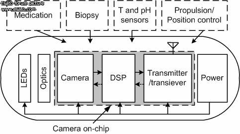
Figure 13. The swalable capsule architecture.
In the dashed boxes additional functionality that will be required in the future is shown
4.2 Artificial Retina
Artificial vision is another example of CMOS image sensors implementation in medical applications. Today
millions of people are suffering from full or partial blindness that was caused by various retinal deceases. In the
early eighties it was shown that electrical stimulation of the retinal nerves can simulate visual sensation even in
the patients with fully degraded receptors. Recently, researchers in a number of research institutes have
developed miniature devices that can be implanted into the eye and stimulate the remaining retinal neural cells,
returning partial vision ability for the blind patients. Such implants are called artificial retinas. Usually they are
implanted in the macula area that normally is densely populated by the receptors and enables high-resolution
vision. This break-through was enabled by the progress in electronics, surgical instrumentation, and
biocompatible materials. Currently there are two major approaches for artificial retina development
(see Figure 14).
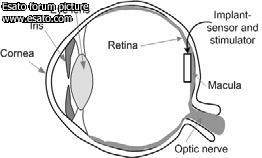
Figure 14. Artificial retinas:
(a) implantable sensor
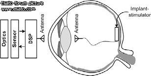
(b) external sensor
The first and the most promising one is the integration of sensing and stimulation elements in the same device
and the second is separation of sensing and stimulation. In the first approach, an artificial retina device is an
autonomous circuitry that does not require external control and the optics that is used for sensing is the natural
optics of the eye composed of the cornea and lens. In the second, all the sensing and processing is performed
outside of the eye and only stimulating elements are implanted during surgery. The data transfer from the sensing
part to the stimulation part is performed through an RF link or through a tiny cable. In both approaches the implant can be subretinal or epiretinal.
Actually there is a number of groups working in the field [40]-[44] but we will concentrate on two that have shown
very promising results and are now performing clinical trials and commercialization through companies named
OptobionicsTM [40] and Second Sight [41]. Both groups already have a number of patients with such implants.
The device developed by OptobionicsTM group does not require any power source, integrates about 5000 sensing
(microphotodiodes) and stimulation (electrodes) elements, features two millimetres in diameter and is implanted
under retina. The basic artificial silicon retina unit is shown in Figure 15 [45]. It is composed of a stimulating
electrode and three PIN photodiodes connected in series to increase the output voltage.
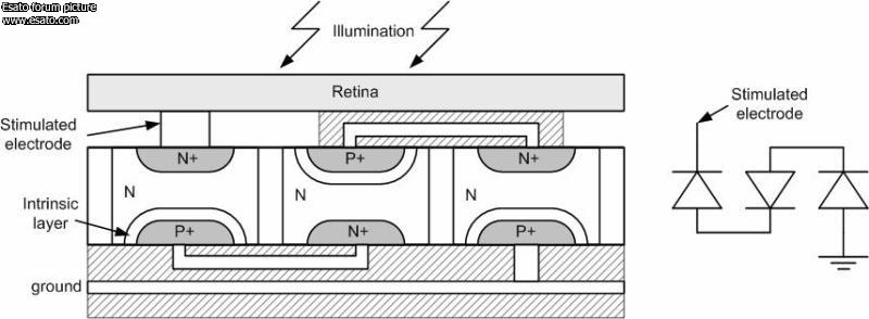
Figure 15. Artificial silicon retina � basic unit
The second group decided to follow the second approach and separate sensing from stimulation. The camera
with the processor is situated on the patient glasses and the signal is transmitted through a cable to the eye that
has an implanted stimulator. Currently, the implant resolution is not so impressive compared to the first group and
features only 16 electrodes, but the developers plan to increase the resolution in the future models to 60 and
1000 electrodes [46].
5. Conclusions
In this paper we have presented a brief review of CMOS image sensors utilization in security and medical
applications. In these applications image sensors play a major role and usually define the edge of the imaging
technology. Despite the CMOS image sensor technology already exists for more than a decade, it is continuously
developing and penetrating into new fields that were unreachable by its predecessor, CCD technology. Although
many successes have been achieved during the last decade, a lot of work still needs to be done in this area. It
requires extensive collaboration between various fields such as: electrical engineering, materials, computer
science, medicine, psychology, chemistry etc. As to the electrical engineering and sensing fields, the work should
be concentrated in the directions of power consumption reduction, functionality improvement and system
integration. However, like in every multidisciplinary, electrical engineers, developing the electronic devices for
medical purposes, are required to understand all above mentioned fields to successfully implement such devices.
References
[1] G. Iddan, G. Meron, A. Glukhovsky, P. Swain, �Wireless capsule endoscopy�, Nature, Vol. 405, p. 417, May 2000
[2] E. Fossum, "Low power camera-on-a-chip using CMOS Active Pixel Sensor technology", in IEEE Symposium on Low
Power Electronics, pp. 74�77, 1995.
[3] O. Yadid-Pecht and R. Etienne-Cummings, "CMOS imagers: from phototransduction to image processing", Kluwer
Academic Publishers, 2004.
[4] A. Fish, D. Turchin, O. Yadid-Pecht, " An APS with 2-Dimensional winner-take-all selection employing adaptive spatial
filtering and false alarm reduction", IEEE Trans. on Electron Devices, Special Issue on Image Sensors, January, 2003.
[5] V. Brajovic and T. Kanade, �Computational sensor for visual tracking with attention�, IEEE journal of solid-state circuits,
Vol.33, No.8, August 1998.
[6] T. Horiuchi and E. Niebur, �Conjunction search using a 1-D, analog VLSI-based attentional search/tracking chip,�
Conference for Advanced Research in VLSI, D. Scott Wills and Stephen P. DeWeerth, Eds., pp. 276�290. IEEE
Computer Society, 1999.
[7] G. Indiveri, �Neuromorphic analog VLSI sensor for visual tracking: Circuits and application examples.� IEEE Trans. On
Circuits and Systems, II 46(11), pp. 1337�1347, November 1999.
[8] C. S. Wilson, T. G. Morris, and P. DeWeerth, �A two-dimensional, object-based analog VLSI visual attention system",
Twentieth Anniversary Conference on Advanced Research in VLSI, IEEE Computer Society Press: Los Alamitos, CA.
Vol. 20. pp. 291-308. March 1999.
[9] M.Clapp and R..Etienne-Cummings, �A dual pixel-type imager for imaging and motion centroid localozation�, Proc.
ISCAS�01, Sydney, Australia, May 2001
[10] N. Mei Yu, T. Shibata and T. Ohmi, �A Real-Time Center-of-Mass Tracker Circuit Implemented by Neuron MOS
Technology�, IEEE transactions on circuits and systems�II, vol. 45, no. 4, April 1998.
[11] R.C. Meitzler, K. Strohbehn and A.G. Andreou, �A silicon retina for 2-D position and motion computation�, Proc.
ISCAS�95, New York, USA, 1995.
[12] A. Simoni, G. Torelli, F. Maloberti, A. Sartori, S. E. Plevridis and A. N. Birbas, �A Single-Chip Optical Sensor with
Analog Memory for Motion Detection�, IEEE Journal of Solid-State Circuits, Vol. 30, No. 7, July 1995.
[13] M. Clapp and R. Etienne-Cummings, �Dual Pixel Array for Imaging, Motion Detection and Centroid Tracking,� IEEE
Sensors Journal, Vol, 2, No. 6, pp. 529-548, December 2002.
[14] S. Kawahito, M. Yoshida, M. Sasaki, K. Umehara, D. Miyazaki, Y. Tadokoro, K. Murata, S. Doushou, and A.
Matsuzawa, �A CMOS Image Sensor with Analog Two-Dimensional DCT-Based Compression Circuits for One-Chip
Cameras�, IEEE Journal of Solid-State Circuits, Vol. 32, No. 12, 1997.
[15] K. Aizawa, H. Ohno, Y. Egi, T.Hamamoto, M. Hatory, H. Maruyama and J. Yamazaki �On sensor Image Compression,�
IEEE Transaction On Circuits And Systems For Video Technology, vol 7, no. 3, pp. 543-548, June 1997.
[16] O. Yadid-Pecht, A. Belenky " In-Pixel Autoexposure CMOS APS " IEEE Journal of Solid-State Circuits, Vol. 38, No. 8,
pp. 1425-1428, August 2003.
[17] A. Fish, A. Belenky and O. Yadid-Pecht, �Wide Dynamic Range Snapshot APS for Ultra Low-Power Applications, IEEE
Transactions on Circuits and Systems II, vol. 52, no. 11, pp. 729-733, November, 2005.
[18] O. Yadid-Pecht, C. Clark, B. Pain, C. Staller, E. Fossum , Wide dynamic range APS star tracker, in Proc. SPIE/IS&T
Sym. on Electronic Imaging: Science and Technology, San Jose, California, SPIE Vol. 2654, Jan 29-Feb3, 1996,
pp. 82-92.
[19] O. Yadid-Pecht, E. Fossum, "Wide Intrascene Dynamic Range CMOS APS Using Dual Sampling" , IEEE Trans. Elec.
Dev., special issue on solid state image sensors, Vol. 44, No. 10, pp. 1721-1724, October 1997.
[20] O. Yadid-Pecht, "Wide dynamic range sensors", Optical Engineering, Vol. 38, No. 10, pp.1650-1660, October 1999.
[21] K. Buckley, "Selecting an Analog Front-End for Imaging Applications", Analog Dialogue, vol. 34-6, pp. 1-5, 2000.
[22] D.X.D. Yang, A. El Gamal, B. Fowler and H. Tian, �A 640x512 CMOS Image Sensor with Ultra Wide Dynamic Range
Floating Point Pixel Level ADC,� IEEE ISSCC, WA 17.5, 1999.
[23] B. Pain, S. Mendis, R. Scober, R. Nixon, and E. Fossum, "Low-power low-noise analog circuits for on-focal-plane
signal processing of infrared sensors," IEEE Workshop on Charge Coupled Devices and Advanced Image Sensors,
June, 1995.
[24] A. Dickinson, S. Mendis, D. Inglis, K. Azadet, and E. Fossum, "CMOS Digital Camera with Parallel Analog-to Digital
Conversion Architecture," IEEE Workshop on Charge Coupled Devices and Advanced Image Sensors, April, 1995.
[25] A. Krymski and N. Tu, "A 9-V/Lux-s 5000-Frames/s 512x512 CMOS Sensor," IEEE Trans. Electron Devices, vol. 50 pp.
136-143, Jan. 2003.
[26] S. Smith, J.Hurwitz, M. Torrie, D. Baxter, A. Holmes, M.Panaghiston, R. Henderson, A. Murray, S. Anderson, and P.
Denyer, "A single-chip 306x244-pixel CMOS NTSC video camera," ISSCC Digest of Technical Papers, pp. 170-171,
February 1998.
[27] M. Loinaz, K. Singh, A. Blanksby, D. Inglis, K. Azadet, and B. Acland," A 200mW 3.3V CMOS color camera IC
producing 352x288 24b Video at 30frames/s," ISSCC Digest of Technical Papers, pp 186-169, February 1998.
[28] G. L. Foresti, C. Micheloni, L. Snidaro, P. Remagnino, and T. Ellis, �Active video-based surveillance system�, IEEE
Signal Processing Magazine, pp. 25-37, March 2005.
[29] E. Artyomov, Y. Rivenson, G. Levi, Orly Yadid-Pecht, �Morton (Z) Scan Based Real-Time Variable Resolution CMOS
Image Sensor�, IEEE Transactions on Circuits and Systems for Video Technology, Volume 15, Issue 7, July 2005,
pp. 947 � 952.
[30] A. Jain, L. Hong, S. Pankanti, �Biometric identification�, Communications of the ACM, Vol. 43, No. 2, 2000.
[31] K. Uchida, �Fingerprint identification�, NEC Journal of Advanced Technology, Vol. 2, No. 1, pp. 19-27, 2005.
[32] S.J. Kim, K.H. Lee, S.W. Han, and E. Yoon, "A 200�160 Pixel CMOS Fingerprint Recognition SoC with Adaptable
Column-Parallel Processors,", IEEE International Solid-State Circuits Conference (ISSCC), pp. 250-251,
February 2005.
[33] �Robotics road map�, EURON Technology Roadmaps, April 23, 2004,
www.org.id.tue.nl/IFIP-SG16/robotics-roadmap-2004.pdf
[34] S. Shigematsu, H. Morimura, Y. Tanabe, T. Adachi, and K. Machida, �A Single-Chip Fingerprint Sensor and Identifier�,
IEEE JOURNAL OF SOLID-STATE CIRCUITS, Vol. 34, No. 12, pp. 1852-1859, December 1999
[35] www.givenimaging.com
[36] www.rfnorika.com
[37] K.N.C. Hin, O. Yadid-Pecht, M. Mintchev, �e-Stool: Self-Stabilizng Capsule for Colonic Imaging�, Neuro-stimulation
Conf, France, July 2005.
[38] microsystem.re.kr/main_eng/menu04/sub_menu01.asp
[39] �Olympus Launches High-resolution Capsule Endoscope in Europe�, Olympus press release, October 13, 2005,
www.olympus.co.jp/en/news/2005b/nr051013capsle.cfm
[40] www.optobionics.com
[41] www.2-sight.com
[42] www.eye-chip.com
[43] www.iip-tec.com/
[44] www.bostonretinalimplant.org/
[45] U.S. Patent US-007003354-B2, given to OptobionicsTM
[46] S. Derra, �Bring sight to the blind�, R&D magazine, 2005, www.rdmag.com
Authors� Information
Evgeny Artyomov � e-mail: artemov@bgu.ac.il
Alexander Fish � e-mail: afish@ee.bgu.ac.il
Orly Yadid-Pecht � e-mail: oyp@ee.bgu.ac.il
The VLSI Systems Center, Ben-Gurion University, Beer Sheva, Israel
MANOMETRY-BASED COUGH IDENTIFICATION ALGORITHM
Jennifer A. Hogan, Martin P. Mintchev
Abstract: Gastroesophageal reflux disease (GERD) is a common cause of chronic cough. For the diagnosis and
treatment of GERD, it is desirable to quantify the temporal correlation between cough and reflux events. Cough
episodes can be identified on esophageal manometric recordings as short-duration, rapid pressure rises. The
present study aims at facilitating the detection of coughs by proposing an algorithm for the classification of cough
events using manometric recordings. The algorithm detects cough episodes based on digital filtering, slope and
amplitude analysis, and duration of the event. The algorithm has been tested on in vivo data acquired using a
single-channel intra-esophageal manometric probe that comprises a miniature white-light interferometric fiber
optic pressure sensor. Experimental results demonstrate the feasibility of using the proposed algorithm for
identifying cough episodes based on real-time recordings using a single channel pressure catheter. The
presented work can be integrated with commercial reflux pH/impedance probes to facilitate simultaneous 24-hour
ambulatory monitoring of cough and reflux events, with the ultimate goal of quantifying the temporal correlation
between the two types of events.
Keywords: Biomedical signal processing, cough detection, gastroesophageal reflux disease.
ACM Classification Keywords: I.5.4 Pattern Recognition: Applications � Signal processing; J.3 Life and Medical
Sciences
_________________
http://brazukas.wordpress.com/
http://picasaweb.google.com/brazzukas
[ This Message was edited by: brazuka on 2008-01-08 12:02 ] | |
|
brazzuka's
Joined: Nov 14, 2007
Posts: > 500
From: South World-Antartida-Sweden
PM, WWW
|
On 2008-01-08 00:26:35, drvodka wrote:
I see you uploaded a newer driver, with some changes. Unfortunately, now the camera doesn't work correctly. I made a video to explain what happens, it's difficult for me to explain such a thing not in my mother language.
First, I try to take a picture, but the camera shows a green screen, then hangs and closes. Then, I change drivers back to 5.30's, and it works.
http://rapidshare.com/files/82080378/MVI_0580proc.avi.html
drvodka
Must be the change in frequency that the camera shows green screen then the hardware k510 works with high frequency like as 48 mhz why??? because the same chips.. i don�t know!!! hahaha #$#@$ crazy hardware.
Well do u r argentine ? so speak in your language spanish , because a little spanish or brazilian if u know , wherever.
O display esta verde por causa da frequ�ncia , ent�o o hardware do k510 trabalha funciona com frequ�ncia acima de 27 mhz com 48 mhz mas n�o entendo porque???? se o chip � o mesmo, ent�o o hardware se comporta de outra forma trabalhando com uma frequ�ncia de 48 mhz.
See u
Correction Fix frequency change by 48 mhz
test the driver
_________________
http://brazukas.wordpress.com/
http://picasaweb.google.com/brazzukas
[ This Message was edited by: brazuka on 2008-01-08 00:29 ]
[ This Message was edited by: brazuka on 2008-01-08 21:39 ] |
gshankar_9
Joined: Jan 07, 2008
Posts: 1
PM |
Hi,
How to install Dat file in W200I,tell me the procidure. |
brazzuka's
Joined: Nov 14, 2007
Posts: > 500
From: South World-Antartida-Sweden
PM, WWW
|
On 2008-01-08 12:54:45, gshankar_9 wrote:
Hi,
How to install Dat file in W200I,tell me the procidure.
*.dat
camdriver0.dat
folder: ifs/settings/camera/camdriver0.dat
|
brazzuka's
Joined: Nov 14, 2007
Posts: > 500
From: South World-Antartida-Sweden
PM, WWW
|
Electronic Manufacture Technologies
Agilent ADCM-2650-0001
Portrait VGA Resolution
CMOS Camera Module
Description
The ADCM-2650-0001 ultra compact CMOS camera module is an advanced, low power VGA resolution camera component for embedded applications. The camera module combines an Agilent CMOS image sensor and image processing design with a high quality lens to deliver images in JPEG or video format.The ADCM-2650-0001 camera module features exceptional low light sensitivity, providing excellent image quality in low
light environments. The camera module is a fully integrated solution � no external
components are required, reducing design complexity and extending design flexibility.
The ADCM-2650-0001 camera module features a quality, integral lens in a tightly
integrated image sensor and image processing design. The camera module is optimized for
use in a variety of embedded applications, from cell phones to image-enabled appliances and automotive design.
The ADCM-2650-0001 cameramodule also supports a range of programmable modes, including support for embedded or external synchronization capabilities.
Features
� 480 x 640 portrait VGA
resolution
� 24 bit color depth (16 million
colors)
� Bayer color filters � blue, red
and green
� Frame rate � 15 fps at VGA
resolution
�Flexible orientation
� Programmable to many image
formats:
-VGA (480 x 640) portrait only
-CIF (352 x 288)
-QVGA (320 x 240)
-QCIF (176 x 144)
-QQVGA (160 x 120)
-QQCIF (88 x 72)
-Any other format 480 x 640 or
smaller
� Panning � window can be
placed anywhere in the 480 x
640 array
� Low power � 120 mW typical at
13 MHz input clock
� High intrinsic sensitivity for
enhanced low light
performance
� Optimized temperature
performance
� Single 2.8V power supply with
internal voltage regulation
� High quality F/2.8 lens
� Direct JPEG, RGB, YUV or
YCbCr 8-bit parallel output
port (CCIR 656-compatible)
� Embedded synchronization
capability � CCIR 656
� Horizontal/vertical mirroring
and subsampling
� Excellent image quality � JPEG
based compression with
automatic or selectable
quantization tables
� Automatic gathering of frame
statistics including histograms
for each color channel
� Integrated PLL and voltage
regulators
� Fully configurable image
processing
� Automatic adjustment of
compression rate for constant
image file size
� Auto exposure and auto white
balance
� Integrated IR filter
� Compact size � 12.5 x 10.5 x 8.2
mm with cover glass
Applications
�Mobile phones
� Video phones
� Personal Digital Assistants
� Image-enabled appliances
� Digital still mini cameras
�Embedded automotive
�Monitoring equipment
Block Diagram
The ADCM-2650-0001 camera module is a complete image processing system.
Agilent
www.agilent.com/semiconductors
|
drvodka
Joined: Jan 07, 2008
Posts: 19
From: Buenos Aires, Argentina.
PM |
drvodka
Must be the change in frequency that the camera shows green screen then the hardware k510 works with high frequency like as 48 mhz why??? because the same chips.. i don�t know!!! hahaha #$#@$ crazy hardware.
Well do u r argentine ? so speak in your language spanish , because a little spanish or brazilian if u know , wherever.
O display esta verde por causa da frequ�ncia , ent�o o hardware do k510 trabalha funciona com frequ�ncia acima de 27 mhz com 48 mhz mas n�o entendo porque???? se o chip � o mesmo, ent�o o hardware se comporta de outra forma trabalhando com uma frequ�ncia de 48 mhz.
See u
Correction Fix frequency change by 48 mhz
test the driver
--------------------------------------------------------------------------------------------
I'm argentine, yes  I was just speaking in english because everybody here does, from here on I'll speak spanish, as you wish. I understand portuguese a bit, but don't expect me to speak or write it, hehe. I was just speaking in english because everybody here does, from here on I'll speak spanish, as you wish. I understand portuguese a bit, but don't expect me to speak or write it, hehe.
Acabo de probar el nuevo driver, y sigo con el problema de la pantalla verde que le he mostrado en el video, solo que esta vez, se nota que la c�mara responde mejor, o sea, toma im�genes m�s seguido que con el driver anterior.
De a poco se lo va mejorando, si, pero sinceramente parece un driver que no le gusta que lo anden modificando. |
brazzuka's
Joined: Nov 14, 2007
Posts: > 500
From: South World-Antartida-Sweden
PM, WWW
|
--------------------------------------------------------------------------------------------
I'm argentine, yes I was just speaking in english because everybody here does, from here on I'll speak spanish, as you wish. I understand portuguese a bit, but don't expect me to speak or write it, hehe.
Acabo de probar el nuevo driver, y sigo con el problema de la pantalla verde que le he mostrado en el video, solo que esta vez, se nota que la c�mara responde mejor, o sea, toma im�genes m�s seguido que con el driver anterior.
De a poco se lo va mejorando, si, pero sinceramente parece un driver que no le gusta que lo anden modificando.
[/quote]
----------------------------------------------------------------------------------------------------
So then i try to speak in spanish , better , to write in spanish
Algunas cosas pasan en el hardware del modelo k510 y otras en el procesador chip porque son cosas distintas el procesador el los sensores son distintos.
Estaba revisando y hasta ahora yo no s� que empresa la fabrica el modelo del chip para el k510 porque hay una mezcla ahi.Yo supongo que son dos empresas que fabrican el hardware total del k510 una se queda con la parte de sensores chips procesadores y la otra el hardware quizas yo que est� equivocado.
Bueno lo que pasa cuando la pantalla display esta verde es porque una de las causas puede ser la frecuencia que no esta ajustada al hardware esto es el sensor chip procesador no suporta la frecuencia estimulada mismo que el hardware trabaje bien otra cosa puede ser que est� faltando lineas de programacion para complementar esa frecuencia.
Yo agregu� lineas de programaccion con las frecuencias de 14mhz para ver si queda mas estable la pantalla el display y borr� removi una de las secuencias inciales y la secuencia power save mode para inciar la cam porque ya habia una secuencia y creo que sea especifica para el modelo k510
agregados adicionados:
-Set framerate to 14 fps
-start de cam a 13mhz
-trabajando a 48mhz e 24 mhz
removido:
-secuencia incial por ya haber una especifica al modelo k510
-secuencia power save mode por no trabajar o no hacer falta el modelo k510
mi espa�ol es re feo una lastima pero espero que si entienda
Saludos
Obs:Lamentablemente no hay como yo testar el driver porque no tengo el modelo k510 y no es verdad que los drivers sierven para cualquier modelo mismo que sean casi iguales o parecidos, no si puede generalizar por la cosa que escribi arriba cada empresa fabrica su modelo de hardware , sensores chips procesadores y por eso hay una limitaccion inibicion y maxima capacidad que cada modelo soporta.
Solamente los testen iran decir como se comporta el driver y gracias por vos testarlos.
fix bug
new driver
download
|
drvodka
Joined: Jan 07, 2008
Posts: 19
From: Buenos Aires, Argentina.
PM |
Tu espa�ol se entiende perfectamente! De verdad, no tuve un solo problema en interpretar lo que vos escribiste.
Ahora entiendo la causa del problema de la pantalla verde. Lamento desilusionarte, pero el problema sigue, al igual que en el video que puse unos 3 posts arriba.
Vos subiste una versi�n de este driver que no ten�a ese problema, pero no sacaba bien las fotos, me refiero al problema de los blancos que parecen grises, y de los colores invertidos (rojos como verdes, naranjas como amarillos, etc), capaz si volves a revisar ese, seguro se puede hacer algo.
No hay problema, vos sub� la cantidad de drivers que quieras, yo los pruebo, como viste en el video, es solo cambiarle el nombre a un archivo lo que tengo que hacer para probarlos. |
pimp123
Joined: Aug 07, 2004
Posts: 172
PM |
My english i'ts very bad, i'm sorry about it .. On W200, i've tried the versions 3.5 and 7.5 that your camdriver brazuka, the pictures in 3.5 it's very better than other version.. Can you check that?
--------------------------------------------------------------------------------------------
Ahora en espa�ol  , luego de realizar varias pruebas entre ambas versiones (3.5 y 7.5), puedo decir que la calidad de las fotos del 3.5 supera AMPLIAMENTE al 7.5, podrias revisar eso brazuka?? , luego de realizar varias pruebas entre ambas versiones (3.5 y 7.5), puedo decir que la calidad de las fotos del 3.5 supera AMPLIAMENTE al 7.5, podrias revisar eso brazuka??
Saludos y felicitaciones por tu camdriver! |
brazzuka's
Joined: Nov 14, 2007
Posts: > 500
From: South World-Antartida-Sweden
PM, WWW
|
camdriver v 5.5 BrAzUkA�s k510
errors bugs
-display green
-the pics no change
-video with colour green
-white balance
correction fix
-frequency 13mhz start cam power cam on
-frequency clock 48mhz to 24mhz
-add properties for works in frequency 14mhz
Added property:
-AE level
-Brightness
-Contrast
-Sharpening
-Focus test
-AF value test
-Spot Photometry
-Photo metering
-Sequences BrAzUkA�s super cam driver Super Color� for k510
-New Sequence JPEG compression level
-New White Balance
Added property:
-Property LUMA_SET_SS
-New Sequence Gamma
_________________
brazukas.wordpress.com
picasaweb.google.com/brazzukas
brazzukas.4shared.com
[ This Message was edited by: brazuka on 2008-01-10 02:19 ] |
brazzuka's
Joined: Nov 14, 2007
Posts: > 500
From: South World-Antartida-Sweden
PM, WWW
|
On 2008-01-10 03:14:02, pimp123 wrote:
My english i'ts very bad, i'm sorry about it .. On W200, i've tried the versions 3.5 and 7.5 that your camdriver brazuka, the pictures in 3.5 it's very better than other version.. Can you check that?
--------------------------------------------------------------------------------------------
Ahora en espa�ol , luego de realizar varias pruebas entre ambas versiones (3.5 y 7.5), puedo decir que la calidad de las fotos del 3.5 supera AMPLIAMENTE al 7.5, podrias revisar eso brazuka??
Saludos y felicitaciones por tu camdriver!
----------------------------------------------------------------------------------------------------
What is your "tip" model for the driver v7.5 cells telephone mobil k310 or w200?
Que modelo estas utilizando un k310 o un w200?
|
pimp123
Joined: Aug 07, 2004
Posts: 172
PM |
I've a k310@w200 |
brazzuka's
Joined: Nov 14, 2007
Posts: > 500
From: South World-Antartida-Sweden
PM, WWW
|
On 2008-01-10 03:21:59, pimp123 wrote:
I've a k310@w200
----------------------------------------------------------------------------------------------------
// Version 7.5 final BrAzUkA�s
// Optimized for the Sony Ericsson W200 ** Works w200 **
as i said in previous post and in the description of the driver v7.5 working for the w200, it is even if the driver works for the k310 will not have the same income as in w200.The k310 is unresponsive to stimules most of the functions and does not address more adequately same chip being similar or equal to the hardware and sensor k310 are different so the version v7.5 is not appropriate to k310 and the LCD display of the k310 is another circuit board "card" that the w200 are different, tests were made with the same version of drivers and the results were different.
Each hardware and processor chip, sensors responds within their limitations and in this case will have its perfomance depending on the hardware and not the software often is the hardware that predominates.
An example equal to computers and mac apple each computer will respond with your system if it is too loaded or not.
A typical example is the PC with the operating system of Apple Mac OS / X can install the operating system of apple on PCs but is not 100% that the yield will be the same from one apple.
I don�t know if i was quite clear?? am clear? or i can maybe wrong and writing mistake
The version correct for k310 v5.0 for k310
|
brazzuka's
Joined: Nov 14, 2007
Posts: > 500
From: South World-Antartida-Sweden
PM, WWW
|
// Sony Ericsson CamDriver Version 4.2 by BrAzUkA�s for k700
// Version 4.2 BrAzUkA�s
// Optimized for the Sony Ericsson k700 ** Works k700 **
-Super Color� Auto function for k700
-New Power Sequence
-New Frequency clock
pic:http://agustin.typepad.com
|
pimp123
Joined: Aug 07, 2004
Posts: 172
PM |
mmm i'm testing the drivers, 3.5v w200 take pictures with more quality than 5.0 k310 brazuka.. | |
|
Access the forum with a mobile phone via esato.mobi
|


 Posted: 2008-01-08 01:03


